Atomically precise mechanosynthesis of carbon structures on hydrogenated Si(100) by inverted-mode STM
Abstract: The ability to build atomically precise structures on surfaces with complete control over both atomic placement and chemical bonding remains a central challenge in nanoscale fabrication. Here, we demonstrate simultaneous spatial and chemical control over the mechanosynthetic fabrication of carbon structures. Using inverted-mode STM, C$_2$ units are donated from surface-deposited molecules to pre-patterned reactive sites on a hydrogen-passivated Si(100) surface. We demonstrate single-site C$_2$ donation, spatially patterned multi-site C$_2$ donation, and the stepwise assembly of polyyne structures through successive C-C bond formation. Together, these results establish controlled mechanosynthetic donation as a foundational capability for programmable atomically precise fabrication.
Paper Prompts
Sign up for free to create and run prompts on this paper using GPT-5.
Top Community Prompts
Explain it Like I'm 14
What is this paper about?
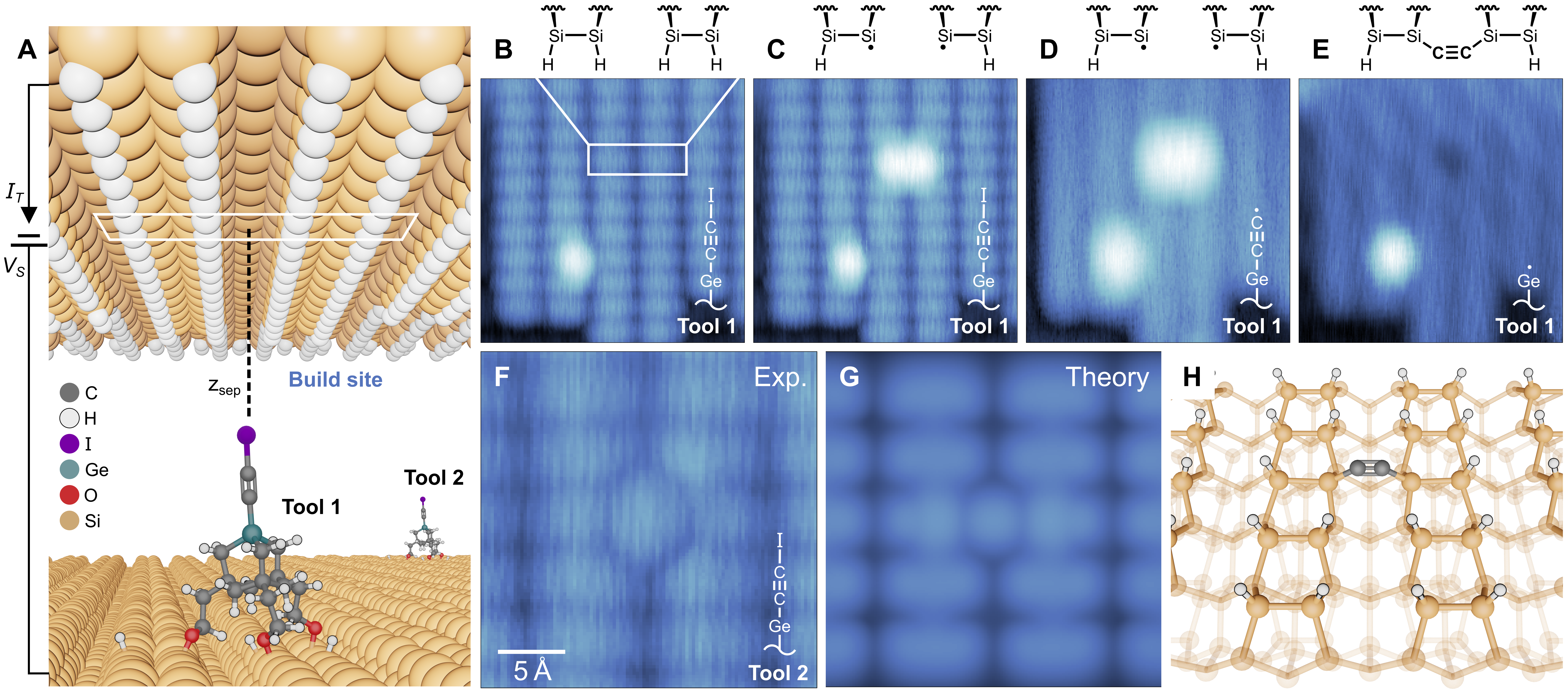
This paper shows a new way to “build with atoms” on a surface, placing tiny pieces of carbon exactly where they’re needed and joining them with the right bonds. The researchers use a special kind of microscope to move and attach pairs of carbon atoms (called C₂ units) onto a silicon surface, one step at a time, with very high control. This is a big step toward making ultra‑small devices, like advanced electronics or parts for quantum computers, by constructing them atom by atom.
What questions were the scientists trying to answer?
In simple terms, they wanted to know:
- Can we put tiny carbon pieces onto a silicon surface exactly where we want them, one atomic site at a time?
- Can we control not just the position of these atoms, but also how they chemically bond to the surface and to each other?
- Can we repeat these steps to build longer carbon chains and patterns in a reliable, programmable way?
How did they do it? (Methods explained simply)
Think of the silicon surface as a flat building board coated with a protective “paint” (hydrogen). Underneath, the silicon has places that can bond—like empty hooks—if you remove the paint at specific spots. These empty hooks are called “dangling bonds.”
The team’s tools and steps:
- The “microscope” they use is a scanning tunneling microscope (STM). Normally, an STM scans a surface with a sharp tip. Here, they use an “inverted-mode” STM, which flips the roles: molecules on the surface act like tiny probes that look upward at a flat silicon chip, which becomes the build site. You can picture this like turning a microscope upside down so the sample helps probe the tool above it.
- Their “molecular tools” are special molecules placed on the surface. Each has:
- A pair of carbon atoms (C₂) ready to be donated like a tiny brick.
- Legs that stick the molecule upright on the surface.
- A cap (iodine) that keeps the C₂ safe until they’re ready to use it.
- First, they make two “dangling bonds” next to each other on the silicon. That’s like removing two spots of paint to reveal two hooks that are ready to bond.
- Next, they remove the iodine cap from the molecular tool to expose a very reactive C₂ “radical”—think of it as a carbon piece eager to grab onto something.
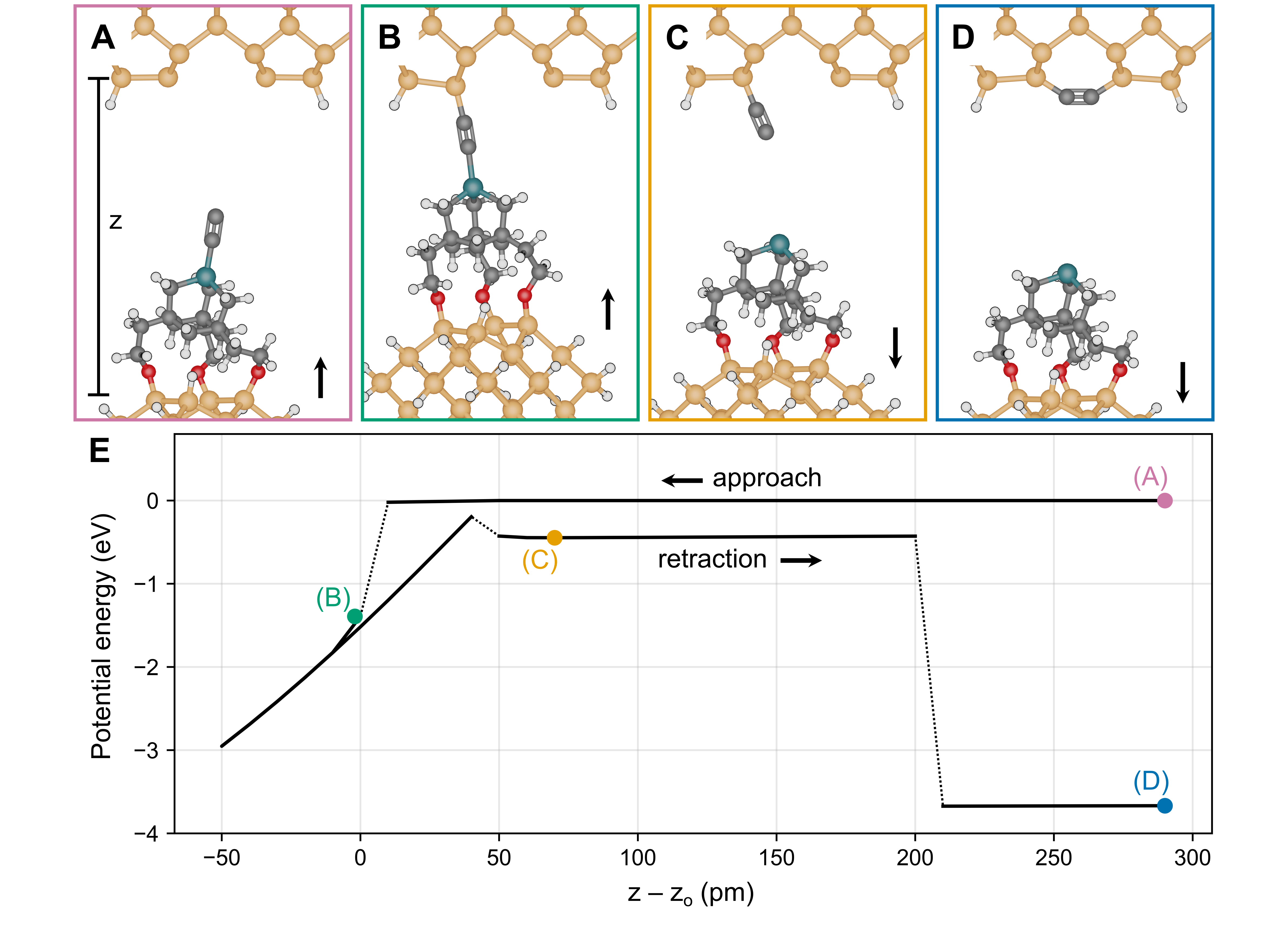
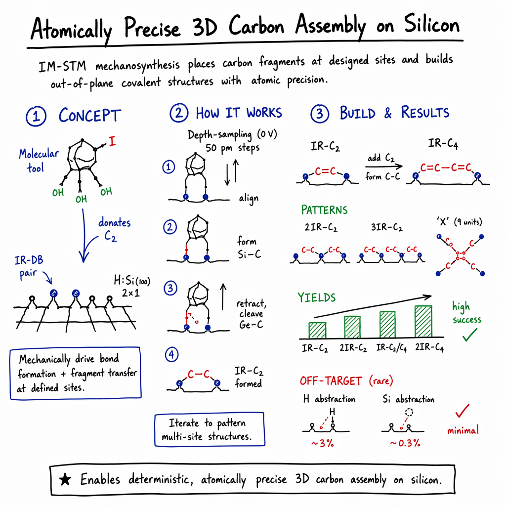
- Then comes the key move: they carefully bring this tool toward the prepared hooks and gently press and release in small steps. This “approach–retract” motion provides mechanical force (like a tiny robotic arm nudging parts together) that: 1) Forms a bond between the carbon and silicon. 2) Breaks the bond holding the C₂ to the tool. 3) Leaves the C₂ attached to the silicon in a well-defined position and shape.
They also use computer simulations (QM/MM) to model the chemistry and energy changes during the process. In everyday terms, that’s like using a physics‑based video game to predict how atoms will move and bond when you push or pull on them.
What did they find, and why does it matter?
Here are the main results:
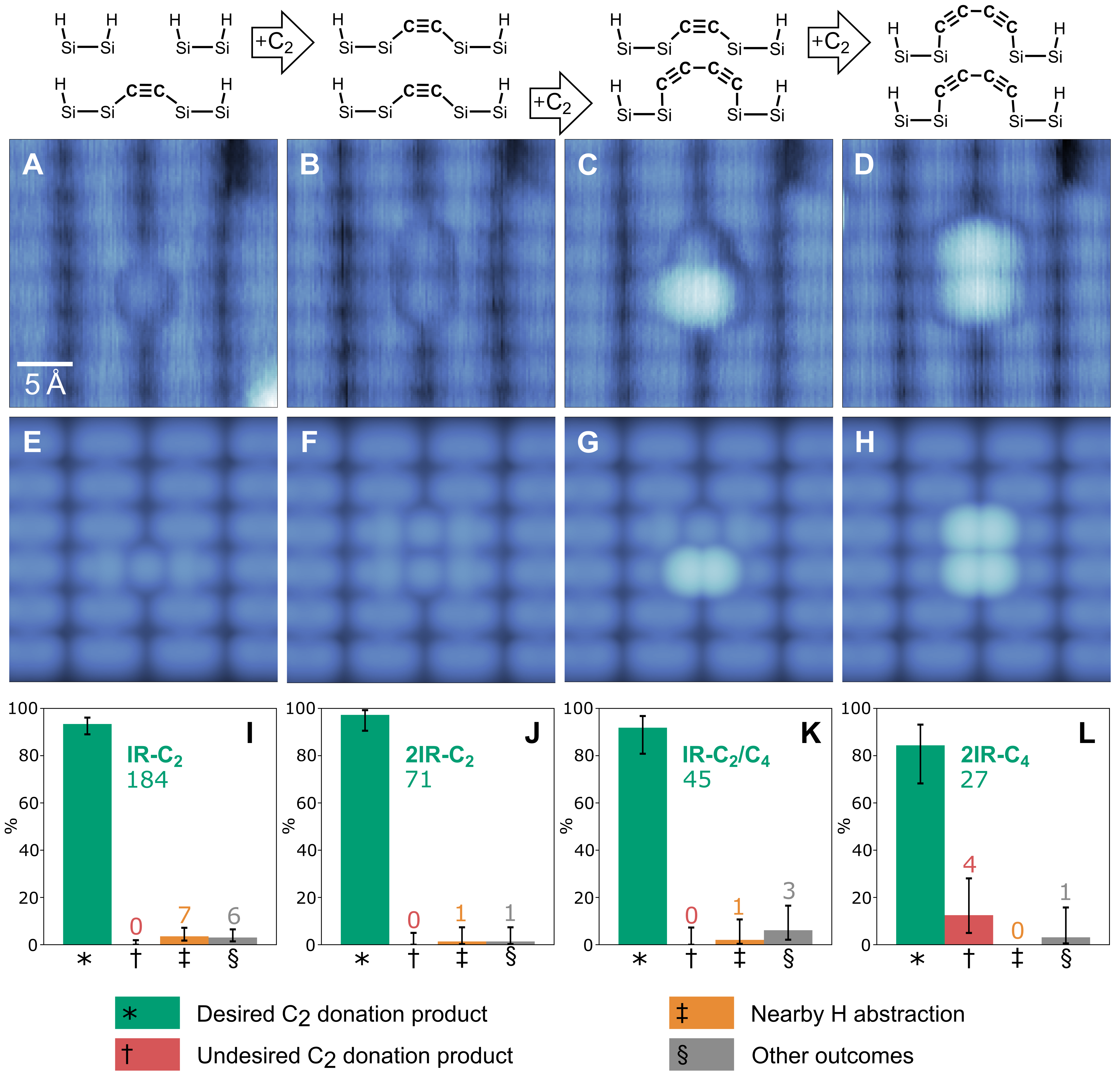
- Single‑site placement: They successfully delivered a C₂ unit to a chosen pair of dangling bonds on hydrogen‑coated silicon, creating a specific structure called “IR‑C₂” (inter‑row C₂). That means precise control over both where the atoms go and how they bond.
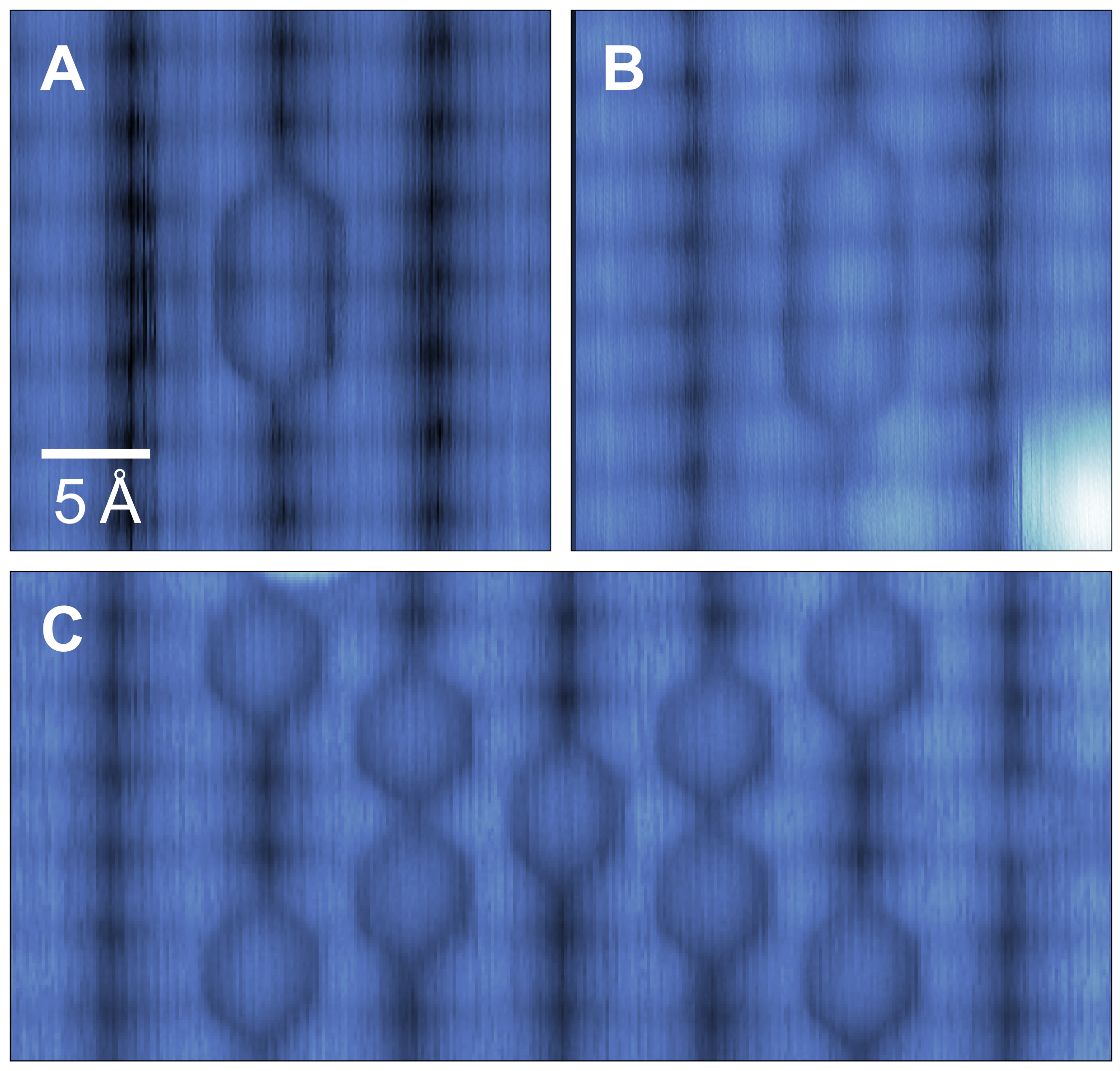
- Patterned placement: By repeating the process, they arranged multiple C₂ units in chosen patterns—side by side along a row and even making shapes like an “X.” This shows they can “draw” with atoms.
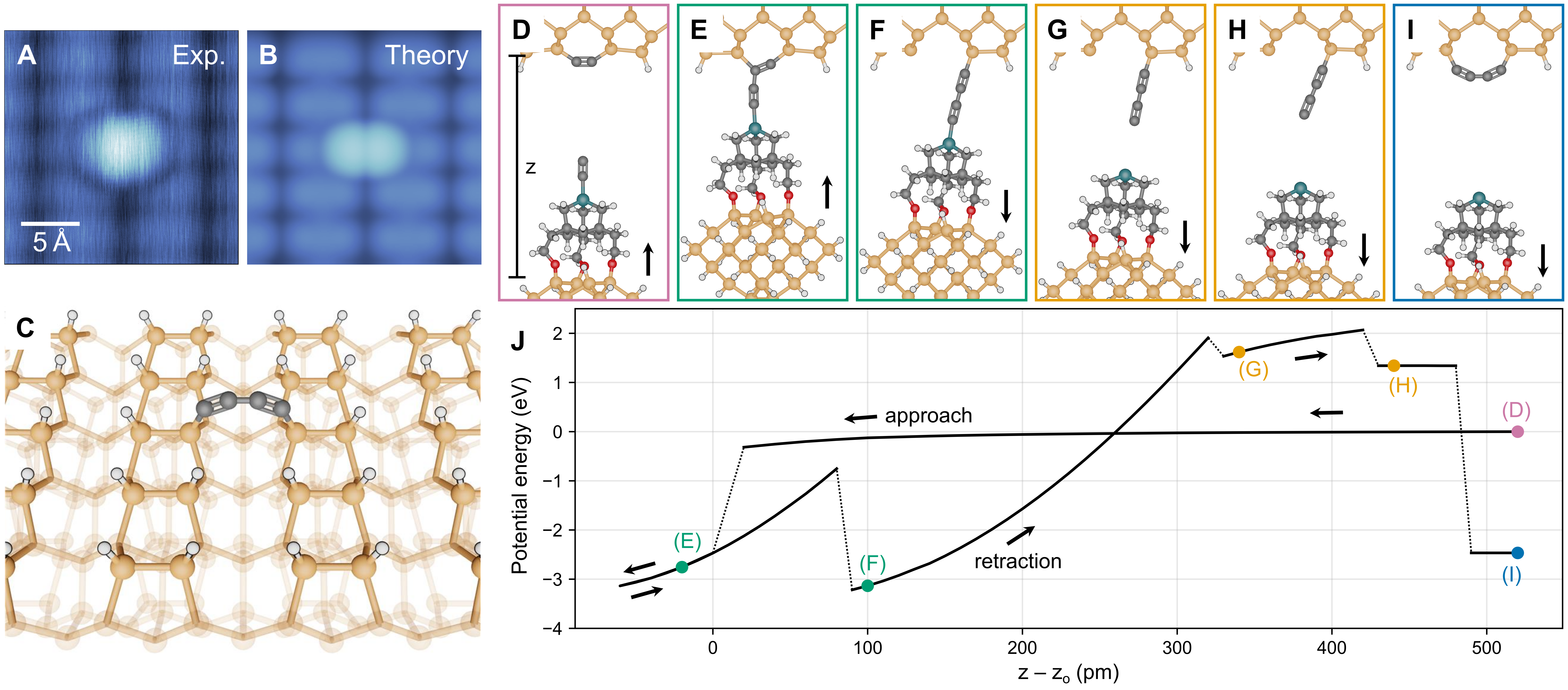
- Stepwise building of longer carbon chains: They didn’t stop at pairs. They added another C₂ onto an existing IR‑C₂ to create a four‑carbon chain (IR‑C₄) through controlled carbon–carbon bond formation. This is like clicking two tiny bricks together to make a longer piece.
- Stability and reproducibility: The built structures stayed intact for days at very cold temperatures (around 4 K, close to absolute zero) and through different imaging settings. They also achieved high success rates across many tries, showing the method is reliable.
- New structures: IR‑C₄ hasn’t been reported before by other methods. This means this technique can create brand‑new, well‑defined atomic structures on surfaces, not just reproduce known ones.
Why it matters: Getting exact control over atom placement and bonding is crucial for building molecular‑scale electronics and parts for quantum devices, where even a single misplaced atom can change how the device behaves. This work shows a programmable way to build in 3D above the surface, not just along it, which is important for realistic device architectures.
What does this mean for the future?
- Programmable atomic manufacturing: These results are a foundation for “atomically precise fabrication,” where devices can be assembled piece by piece with exact instructions, like coding a 3D printer for atoms.
- Better, smaller, and more efficient devices: With atomic‑level control, we can design electronic components that are faster and use less energy, and create new building blocks for quantum technologies.
- New chemistry on surfaces: Mechanically guided bonding opens pathways to structures that are hard or impossible to make with heat or light, expanding the toolbox for surface chemistry and nanotechnology.
- Toward complex 3D architectures: Because they can place and connect carbon units out of the plane of the surface, this approach can help build realistic, layered nanoscale systems directly on silicon, the material behind modern electronics.
In short, this paper shows that we can place and connect tiny carbon parts on silicon with high precision and repeatability, bringing the dream of building functional devices atom by atom closer to reality.
Knowledge Gaps
Knowledge gaps, limitations, and open questions
The paper establishes atomically precise C2 donation and stepwise extension to IR-C4 on H:Si(100) at 4 K using inverted-mode STM (IM-STM), supported by QM/MM mechanisms. The following unresolved issues and gaps remain for future work:
- Temperature robustness and environmental stability: Do IR‑C2 and IR‑C4 remain intact upon warming to 77 K and room temperature, under UHV and in more practical environments (e.g., higher pressure, exposure to residual gases), and through thermal cycling?
- Generality across substrates and passivation: Can the mechanosynthetic donation strategy be extended to other surfaces (e.g., Si(111), Ge(100), diamond, III–V) and passivations (Cl, Br, F), and how do surface reconstructions and band bending affect yields and selectivity?
- Other target site geometries: How do alternative dangling bond (DB) patterns (e.g., intra‑row, different separations, multiple DB motifs) change the product distribution, mechanism, and yield compared to the inter‑row geometry used here?
- Beyond C2 and C4: What are the limits to chain length and complexity (e.g., IR‑C6, IR‑C8, longer polyynes, cross‑linked networks), and how do success rates evolve with step count (error accumulation, failure modes)?
- True out‑of‑plane growth: Can pendent intermediates be captured to form stable vertical (out‑of‑plane) bonds and multilayer structures rather than relaxing into the trough‑bridging IR configuration?
- Heteroatom and functional group transfer: Can the method transfer other fragments (e.g., C1, C3, CN, functionalized C2, N/O/S donors, metal atoms), and what tool design rules govern selectivity and bond formation for these species?
- Electronic and vibrational characterization: Beyond STM contrast, can nc‑AFM, STS, IETS, or Raman/TERS confirm bond order, hybridization (e.g., polyyne vs cumulene character), and local electronic states of IR‑C2/IR‑C4?
- Force and kinetics metrology: What are the quantitative force thresholds and rate dependencies (approach/retract speed, dwell time) for bond formation and cleavage, and how do these correlate with yields and off‑target events?
- Electric field and bias effects: How do applied bias, contact potential difference, and local fields influence initial bond formation, Ge–C vs Si–C bond cleavage competition, and relaxation pathways—even when the nominal bias is set to 0 V?
- Off‑target product identification: The reproducible non‑IR product observed during 2IR‑C4 attempts remains ambiguous; can it be structurally assigned (e.g., via high‑resolution AFM/STS) and mechanistic pathways (tool binding to IR‑C4 vs cross‑coupling of a pendent C4•) be distinguished?
- Mitigating H‑abstraction (≈3%): What modifications (e.g., deuteration of passivation, altered approach trajectories, stiffer tool linkers, different passivants) most effectively suppress unintended H abstraction attributed to lateral flexibility and/or hydrogen tunneling?
- Tool design and reusability: How do leg binding configurations, rigidity, and the Ge–C linkage strength control lateral targeting tolerance, Ge–C vs Si–C cleavage bias, and tool reuse across multiple operations (post‑donation EAOGe* stability, refunctionalization)?
- SPC apex variability: How sensitive are outcomes to the atomic structure, flatness, and contamination of the silicon probe chip (SPC) apex, and what in situ metrology and conditioning protocols minimize device‑to‑device variation?
- Patterning density and cross‑talk: What are spacing limits and orientations that avoid cross‑reactions between adjacent IR‑C2/C4 units, and how does local pattern density affect yields, particularly for multi‑site and multi‑step sequences?
- Error propagation and repair: How do rare off‑target products and isolated failures compound in longer build sequences, and can deterministic “repair” operations (e.g., re‑passivation, selective removal) be integrated into protocols?
- Automation and throughput: What are the time costs and success‑rate trade‑offs for step size (50 pm here), approach/retract rates, and real‑time event detection, and can closed‑loop automation or parallel tool arrays increase throughput for larger patterns?
- Yield sensitivity to parameters: Systematic maps of yield vs approach depth, increment size, lateral alignment tolerance, and tool orientation are not provided; what parameter windows maximize selectivity for each reaction step?
- Integration with device functionality: How do IR‑C2/C4 affect local conductivity, charge trapping, and coupling to dopants or quantum states in Si, and can these carbon features be electrically addressed or integrated with gates/contacts?
- Long‑term stability under operation: Do repeated imaging and higher‑bias operations (beyond the tested ranges) degrade the structures or induce rearrangements, and how do these structures fare under subsequent processing steps relevant to device fabrication?
- Comprehensive mechanistic energetics: The QM/MM approach (xTB(GFN0)/DFT ωB97X‑D3) provides plausible pathways but lacks periodic slab treatment of the full surface and explicit kinetics; can NEB/MD on periodic DFT models quantify barriers, branching ratios, and temperature effects?
- Ge–C vs Si–C bond strength near‑degeneracy: Given the calculated near‑degeneracy of proxy bond energies, what microscopic factors (strain, local fields, coordination) bias cleavage toward Ge–C during retraction, and can this be tuned predictively?
- Real‑time signatures of bond events: Are there measurable current spikes, force jumps, or Kelvin probe signals during approach/retraction that could serve as feedback triggers to halt at optimal z or to flag off‑pathway events?
- Surface charge and dopant effects: How do DB charge states, substrate doping, and band bending alter reaction energetics and selectivity, and can the method operate reliably across different doping profiles?
- Scope of DB patterning methods: The study mixes electron‑induced desorption and mechanosynthetic H abstraction; what are their respective defect rates, spatial precision limits, and impacts on subsequent donation yields?
- Verification of novel geometries: IR‑C4 is proposed as a new structure; beyond STM simulations, can direct chemical validation (e.g., bond‑resolved nc‑AFM) confirm geometry and bonding to resolve the unobserved nodal feature discrepancy in STM?
- Pathway control to stabilize non‑IR products: Can alternative retraction trajectories or auxiliary fields trap the pendent intermediates to access other binding motifs intentionally, expanding the accessible structure set?
- Tool–surface lateral control: What is the quantitative lateral targeting tolerance window for successful donation to intended sites vs neighboring H sites or carbon structures, and how does this depend on tool design and surface topography?
- Extending to heterogeneous architectures: Can sequential placement of different fragments (e.g., C followed by N/O) produce mixed covalent motifs with controlled bond order and orientation, and what cross‑reactivity constraints arise?
- Process compatibility and contamination: What are the impacts of residual gases, adventitious adsorbates, and iodine byproducts on yields and surface quality over multi‑day operations, and how can in situ cleaning be incorporated?
Practical Applications
Immediate Applications
The following applications can be piloted now in laboratories equipped with UHV and low-temperature scanning probe systems, leveraging the demonstrated inverted‑mode STM (IM‑STM) protocol, C2 donation chemistry, and stepwise patterning on H:Si(100).
- IM‑STM instrument workflows and calibration standards
- Sectors: research instruments, semiconductor R&D, metrology
- Use case: Deploy the iterative depth‑sampling protocol, tool-termination “imaging modality” tracking, and H:Si IR-DB prepatterning to reproducibly place IR‑C2 and IR‑C4 units for instrument qualification and operator training.
- Tools/products/workflows: IM‑STM control software implementing approach–retract depth sampling; silicon probe chips (SPCs) with flat crystalline apex; EAOGe‑C2I “molecular tool” kits; standard “X”-pattern IR‑C2 arrays as calibration artifacts; STM/DFT image libraries for modality recognition.
- Assumptions/dependencies: UHV and 4 K operation; reliable H‑termination and DB creation; access to molecular tools; SPC fabrication capacity.
- Deterministic surface-chemistry testbeds for theory/ML validation
- Sectors: academia, software
- Use case: Benchmark QM/MM and DFT mechanochemistry (e.g., bond formation/cleavage pathways, energy landscapes) against high-yield experimental outcomes; generate labeled datasets to train ML potentials for mechanosynthesis control.
- Tools/products/workflows: Curated datasets (tool terminations, depth trajectories, outcomes); NEB/ASE automation scripts; simulation–experiment comparison pipelines.
- Assumptions/dependencies: Consistent reproducibility; shared data standards and metadata; compute resources.
- Model platforms for silicon–carbon interface physics
- Sectors: semiconductor R&D, quantum devices
- Use case: Pattern IR‑C2/IR‑C4 units near dopants, DB logic elements, or quantum dots to probe local band bending, in-gap states, and electrostatic/gating interactions via STS.
- Tools/products/workflows: Site-specific patterns, STS/AFM spectroscopy, device modeling to correlate structure–function.
- Assumptions/dependencies: Low‑temperature stability (demonstrated); spectroscopic mapping; careful defect control.
- Automated outcome detection and process control
- Sectors: software/automation, research instruments
- Use case: Real-time classification of tool termination and reaction states from IM‑STM contrast to adapt approach depth and suppress off-target H‑abstraction.
- Tools/products/workflows: Lightweight ML classifiers trained on “imaging modality” transitions; closed‑loop control APIs for SPM.
- Assumptions/dependencies: Labeled image sets; controller integration; safety interlocks.
- Education and workforce training in atomically precise fabrication (APF)
- Sectors: education, national labs
- Use case: Hands‑on curricula for APF using reproducible IR‑C2 patterning and extension to IR‑C4; remote labs using recorded data and simulations.
- Tools/products/workflows: Step‑by‑step recipes, simulation-backed labs, assessment via build yields.
- Assumptions/dependencies: Access to cryogenic SPMs (for hands‑on); open educational resources.
- Specialty consumables for APF
- Sectors: chemicals, components
- Use case: Supply chain for EAOGe‑C2I derivatives, alternative fragment donors, SPCs, and prepared H:Si substrates as standardized consumables.
- Tools/products/workflows: Molecule synthesis and QC, SPC wafer processes, packaging for UHV.
- Assumptions/dependencies: IP/licensing; batch-to-batch consistency; safety and storage.
- Nanoscale fiducials for lithography alignment and metrology
- Sectors: metrology, semiconductor R&D
- Use case: Atomically precise, non-volatile fiducials (e.g., IR‑C2 “X” patterns) to align STM/AFM lithography and track drift over days.
- Tools/products/workflows: Pattern libraries, image recognition routines for fiducials.
- Assumptions/dependencies: Cryo stability (demonstrated); integration with existing SPM toolchains.
- Fundamental spectroscopy of sp‑carbon chains on silicon
- Sectors: academia (surface science, physical chemistry)
- Use case: Systematic studies of vibrational/electronic properties and chain‑length effects using IR‑C2/IR‑C4 as stable platforms.
- Tools/products/workflows: STS/IETS/AFM mapping across patterned arrays; comparison to theory.
- Assumptions/dependencies: Low-temperature capability; high SNR spectroscopy.
Long‑Term Applications
These applications will require advances in throughput, temperature robustness, automation, chemistry toolkits, and process integration beyond current 4 K, single‑probe operation.
- Scalable APF of 3D carbon architectures on silicon
- Sectors: semiconductor, molecular electronics
- Use case: Build vertical molecular wires, interconnects, and device primitives by stepwise donation (C1/C2/heteroatom libraries) and out‑of‑plane bonding, integrated with CMOS.
- Tools/products/workflows: Parallel IM‑STM/SPM arrays; robust molecular toolkits; automated recipe compilers; in‑situ verification.
- Assumptions/dependencies: Parallelization to raise throughput; room‑temperature or encapsulated stability; contamination control; yield management.
- Hybrid silicon quantum devices with atomically placed carbon features
- Sectors: quantum computing/sensing
- Use case: Use deterministically placed carbon chains/radicals as qubits, couplers, or tunable charge/spin environments adjacent to donors and quantum dots.
- Tools/products/workflows: Co-design with device electrodes; cryo‑RF readout; patterning around qubit sites; spectroscopic pre‑screening.
- Assumptions/dependencies: Demonstration of coherent states and long T2; reproducible coupling; compatibility with device processing.
- Ultra‑dense atomic memory and logic
- Sectors: data storage, unconventional computing
- Use case: Encode bits in presence/absence or length of IR‑C_n units; exploit out‑of‑plane contrast for robust readout; prototype molecular logic via controlled C–C couplings.
- Tools/products/workflows: Parallel write heads; error-correcting coding; fast readout SPM or alternative sensors.
- Assumptions/dependencies: Room‑temperature retention and read speed; endurance; scalable manufacturing.
- Programmable catalytic and reactive surfaces
- Sectors: energy, chemicals
- Use case: Atomic‑level tuning of active sites by placing carbon/heteroatom motifs on semiconductors or passivated metals to steer reaction pathways (e.g., CO2 reduction, hydrogen evolution).
- Tools/products/workflows: Expanded tool libraries (N/O/S/metal fragments); operando spectroscopy; protective overlayers for ambient operation.
- Assumptions/dependencies: Translation to catalytically relevant substrates/environments; stability under bias/temperature; throughput.
- Nanoscale sensors and NEMS elements
- Sectors: sensors, IoT, healthcare diagnostics
- Use case: Carbon chains as mechanically/electronically responsive elements for chemical/strain sensing at single‑molecule limits.
- Tools/products/workflows: Transduction schemes (tunnel, capacitive, optical); encapsulation layers; CMOS interfacing.
- Assumptions/dependencies: Environmental robustness; reproducible transfer functions; wafer‑scale patterning.
- Designer quantum and topological materials on surfaces
- Sectors: academic materials physics
- Use case: Assemble lattices of carbon features to emulate graphene‑like bands, flat bands, or topological edge states directly on Si for explorations of correlated phenomena.
- Tools/products/workflows: Lattice pattern generators; STS band mapping; theoretical co‑design.
- Assumptions/dependencies: Large‑area pattern uniformity; disorder control; cryogenic measurement.
- Secure hardware primitives and unclonable features
- Sectors: security/defense, fintech
- Use case: Atomically unique, verifiable surface signatures (PUFs) created by controlled yet stochasticized mechanosynthesis for anti‑counterfeiting and secure IDs.
- Tools/products/workflows: Challenge–response readout protocols; cryptographic binding to devices.
- Assumptions/dependencies: Scalable, tamper‑resistant readout; longevity outside UHV; manufacturability.
- Commercial APF process modules for niche, high‑value devices
- Sectors: equipment suppliers, semiconductor
- Use case: IM‑STM process tools as fab modules for prototyping/small‑volume manufacture (e.g., specialized sensors, qubit initializers).
- Tools/products/workflows: Turn‑key IM‑STM systems; reliability/maintenance programs; recipe libraries and certification.
- Assumptions/dependencies: Serviceable uptime; operator training; standards and safety certification.
- Closed‑loop AI for mechanosynthesis
- Sectors: software/automation
- Use case: Reinforcement learning and model‑predictive control to select approach trajectories, lateral targeting, and tool chemistries that maximize yield and speed.
- Tools/products/workflows: Large multimodal datasets; physics‑informed RL; digital twins; uncertainty‑aware control.
- Assumptions/dependencies: High‑fidelity simulators; safe exploration; robust sensors.
- Cross‑substrate generalization
- Sectors: materials, electronics
- Use case: Extend controlled donation to H‑passivated Ge(100), diamond, h‑BN, and 2D materials to broaden device platforms.
- Tools/products/workflows: Passivation/DB creation methods per substrate; adapted tool chemistries; comparative mechanistic studies.
- Assumptions/dependencies: Favorable binding energetics; stable intermediates; substrate‑specific process windows.
- Molecular tool ecosystem and on‑surface synthetic chemistry
- Sectors: chemicals, pharma discovery (methodology), advanced materials
- Use case: Libraries of transferable fragments (C1/C2/heteroatoms/functional groups) enabling stepwise, programmable on‑surface synthesis of bespoke molecules/polymers with positional control.
- Tools/products/workflows: Modular tool synthesis; de‑protection/de‑capping strategies; sequence planners; in‑situ verification.
- Assumptions/dependencies: Selectivity across a broader reaction set; intermediate stability; expanded reaction grammar.
- Remote and distributed APF education platforms
- Sectors: education, workforce development
- Use case: Cloud‑connected IM‑STM sessions and high‑fidelity simulators delivering APF training at scale.
- Tools/products/workflows: Digital twins; streamed datasets; competency assessments tied to build yield and error analysis.
- Assumptions/dependencies: Cost-effective access; curriculum partnerships; instrument time sharing.
Notes on key global dependencies and risks
- Temperature: Current demonstrations are at 4 K; many applied use cases require room‑temperature stability or encapsulation strategies.
- Throughput: Single‑probe SPM is slow; meaningful industrial impact requires parallelization (probe arrays) and high automation.
- Chemistry breadth: Today’s EAOGe‑C2I tools provide C2 donation; broader fragment libraries and robust de‑capping chemistries are needed for complex device structures.
- Process integration: UHV/cryogenic constraints must be reconciled with CMOS lines, packaging, and field operation.
- Verification/readout: Application‑specific metrology (fast, non‑contact readout, electrical integration) is required to translate patterns into functioning devices.
Glossary
- 2×1 reconstruction: A surface reconstruction of Si(100) where surface atoms form dimer rows in a 2-by-1 pattern. "The build sequence begins on an H-terminated, 2\texttimes1-reconstructed Si(100) (H:Si) surface (Fig. 1B)."
- adamantane: A rigid, cage-like hydrocarbon used as a molecular scaffold. "The molecular tool used here, EAOGe-CI, consists of a Ge-substituted adamantane with a C functional group, three OH-terminated legs, and an iodine capping group"
- adsorbate: An atom or molecule attached to a surface via adsorption. "including lifting and repositioning of adsorbates and transfers of individual atoms"
- approach-retraction cycles: Repeated vertical motions to bring a probe towards and away from a surface during mechanosynthesis. "Mechanosynthesis is then carried out using iterative depth sampling with repeated approach-retraction cycles from a large initial separation."
- atomically precise fabrication (APF): Bottom-up construction with deterministic atomic placement and bonding on surfaces. "Atomically precise fabrication (APF) seeks to realize this level of control through atom-by-atom operations within a fixed reference frame, typically on a surface."
- bias pulsing: Applying short voltage pulses to induce site-specific surface reactions or desorption. "two Si dangling bonds (DBs) are patterned by bias pulsing in an inter-row (IR) configuration (C)"
- dangling bond (DB): An unsatisfied valence on a surface atom that acts as a reactive site. "A single silicon dangling bond (DB) is present near the target area;"
- de-iodination: Removal of an iodine atom from a molecule to expose a reactive site. "Tool 1 is de-iodinated away from the build site by increasing the bias"
- dehydrogenation: Removal of hydrogen atoms from a molecule or surface. "via de-hydrogenation of adsorbed acetylene and ethylene"
- density functional theory (DFT): A quantum mechanical method for computing electronic structure and energies. "QM/MM xTB(GFN0)/DFT (B97X-D3) simulation illustrating the proposed mechanosynthetic IR-C donation mechanism."
- dimer row: A row of paired surface atoms (dimers) on reconstructed Si(100). "two and (B) three IR-C units patterned side-by-side along a dimer row"
- diyne: A carbon chain containing two triple bonds (–C≡C–C≡C–). "rearranging into a four-carbon diyne intermediate bound to both the Si surface and the molecular tool (Fig. 4F)."
- EAOGe-C2I: A specific Ge-substituted adamantane-based molecular tool bearing a C2 group and an iodine cap. "The molecular tool used here, EAOGe-CI, consists of a Ge-substituted adamantane with a C functional group, three OH-terminated legs, and an iodine capping group"
- electron-induced desorption: Removal of atoms (e.g., H) from a surface via electron-stimulated processes. "DB formation follows the established electron-induced desorption mechanism"
- filled-state STM: Imaging mode/simulation emphasizing occupied electronic states in STM. "a filled-state STM simulation of IR-C (Fig. 1G) closely matches the experimental image"
- H-abstraction: Removal of a hydrogen atom by forming a new bond with a reactive species. "This H-abstraction pathway was observed in nine out of the 351 total interactions shown in Fig. 5"
- hydrogen passivation (H-passivated): Terminating surface dangling bonds with hydrogen to render the surface inert. "an H-passivated Si(100) silicon probe chip (SPC) with a flat, crystalline apex is positioned above the surface."
- IM-STM (inverted-mode scanning tunneling microscopy): An STM mode where surface-bound molecules image a probe chip apex and mediate transfers. "Mechanosynthesis was performed using invertedâmode scanning tunneling microscopy (IMâSTM) operated at 4~K, following \cite{Barrera2025}."
- inter-row (IR) configuration: A geometry spanning the trough between dimer rows on Si(100). "A DB pair is created in an inter-row (IR) configuration (spanning a trough of the reconstructed H:Si surface)"
- IR-C2: A C2 fragment bound in the inter-row geometry on Si(100). "The image reveals a new feature in the target area, which is assigned to C in an IR configuration (IR-C)."
- IR-C4: A C4 chain bound in the inter-row geometry on Si(100). "The resulting feature is assigned to a fourâcarbon chain in an IR configuration (IRâC)."
- IR-DB pair: Two adjacent dangling bonds patterned in an inter-row geometry. "EAOGe-Câ¢) is positioned with the distal C atom centred under an IR-DB pair (Fig.~3A)."
- mechanosynthesis: Directing chemical reactions by mechanically positioning reactive species rather than using thermal/electronic excitation. "Positionally controlled mechanosynthesis offers a route to this goal"
- molecular tool: A surface-bound molecule serving both as an imaging probe and a reactive agent for mechanosynthesis. "The dual functionality of these molecules â as imaging probes and chemical reactants â is the basis for referring to them as \"molecular tools\"."
- pendent radical: A temporarily surface-attached radical fragment hanging from a single bond before final rearrangement. "producing an upright, surface-bound pendent C⢠intermediate"
- polyyne: A linear sp-hybridized carbon chain with alternating single and triple bonds. "the stepwise assembly of polyyne structures through successive C-C bond formation."
- QM/MM (quantum mechanics / molecular mechanics): A multiscale simulation approach combining quantum and classical models. "Figure 1 shows a proposed C donation mechanism, based on a quantum mechanics / molecular mechanics (QM/MM) model"
- scanning probe microscopy (SPM): Techniques using a nanoscale probe to image/manipulate surfaces (e.g., STM/AFM). "Scanning probe microscopy (SPM) is an established platform for pursuing APF"
- scanning tunneling microscopy (STM): A scanning probe method where tunneling current images/controls surfaces at atomic scale. "Mechanosynthesis was performed using invertedâmode scanning tunneling microscopy (IMâSTM) operated at 4~K"
- Si(100): The silicon surface oriented along the (100) crystal plane. "flat Si(100), and an H-passivated Si(100) silicon probe chip (SPC) with a flat, crystalline apex is positioned above the surface."
- silicon probe chip (SPC): A flat, crystalline silicon chip that acts as the imaging/build substrate in IM-STM. "the apex of a large, flat silicon probe chip (SPC)"
- sp3 hybridization: Tetrahedral bonding configuration typical of saturated carbon or silicon centers. "the preferred sp hybridization geometry of the anchoring Si atom"
- tunneling current: The quantum current flowing between probe and sample at small bias/gap in STM. "where an applied bias (V\textsubscript{S}) drives a tunneling current (I\textsubscript{T}) through the molecule"
- vertical transfer: Mechanically driven movement of atoms/fragments between tool and surface along the surface normal. "extending these structures through successive CâC bond formation by vertical transfer of an additional C."
- vinyl radical: A carbon-centered radical on an sp2 carbon within a vinyl group. "resulting in the formation of an intermediate vinyl radical (Fig. 4E)."
- Wilson score: A method for estimating confidence intervals for binomial proportions. "error bars indicate 95\% confidence intervals computed using the Wilson score."
- xTB(GFN0): A semiempirical tight-binding quantum method (GFN0 parametrization) used within QM/MM. "QM/MM xTB(GFN0)/DFT (B97X-D3) simulation illustrating the proposed mechanosynthetic IR-C donation mechanism."
- ωB97X-D3: A range-separated hybrid DFT functional with dispersion corrections. "QM/MM xTB(GFN0)/DFT (B97X-D3) simulation illustrating the proposed mechanosynthetic IR-C donation mechanism."
Collections
Sign up for free to add this paper to one or more collections.

