- The paper introduces a 3D NAND-centric architecture that offloads FFN computation to NAND Flash, addressing memory bandwidth bottlenecks in edge LLM inference.
- It employs wafer-to-wafer integration and out-of-order pipelining with error-resilient dot-product engines to achieve up to 37.9× throughput and 28.2× latency reductions.
- The architecture minimizes energy consumption and area overhead, enabling efficient INT8/BF16 processing for large-scale models on resource-constrained devices.
NVLLM: 3D NAND-Centric Architecture for On-Device LLM Inference
Introduction and Motivation
NVLLM introduces a 3D NAND-centric system architecture specifically attuned to the unique demands of LLM inference on edge devices, where workload characteristics and resource constraints fundamentally diverge from cloud-centric deployments. On-device LLM inference is dominated by single-batch, single-token decodes imposed by interactive usage patterns. Under these conditions, memory bandwidth—rather than compute—emerges as the primary bottleneck, as evidenced by comprehensive roofline analyses and conversation-trace statistics.
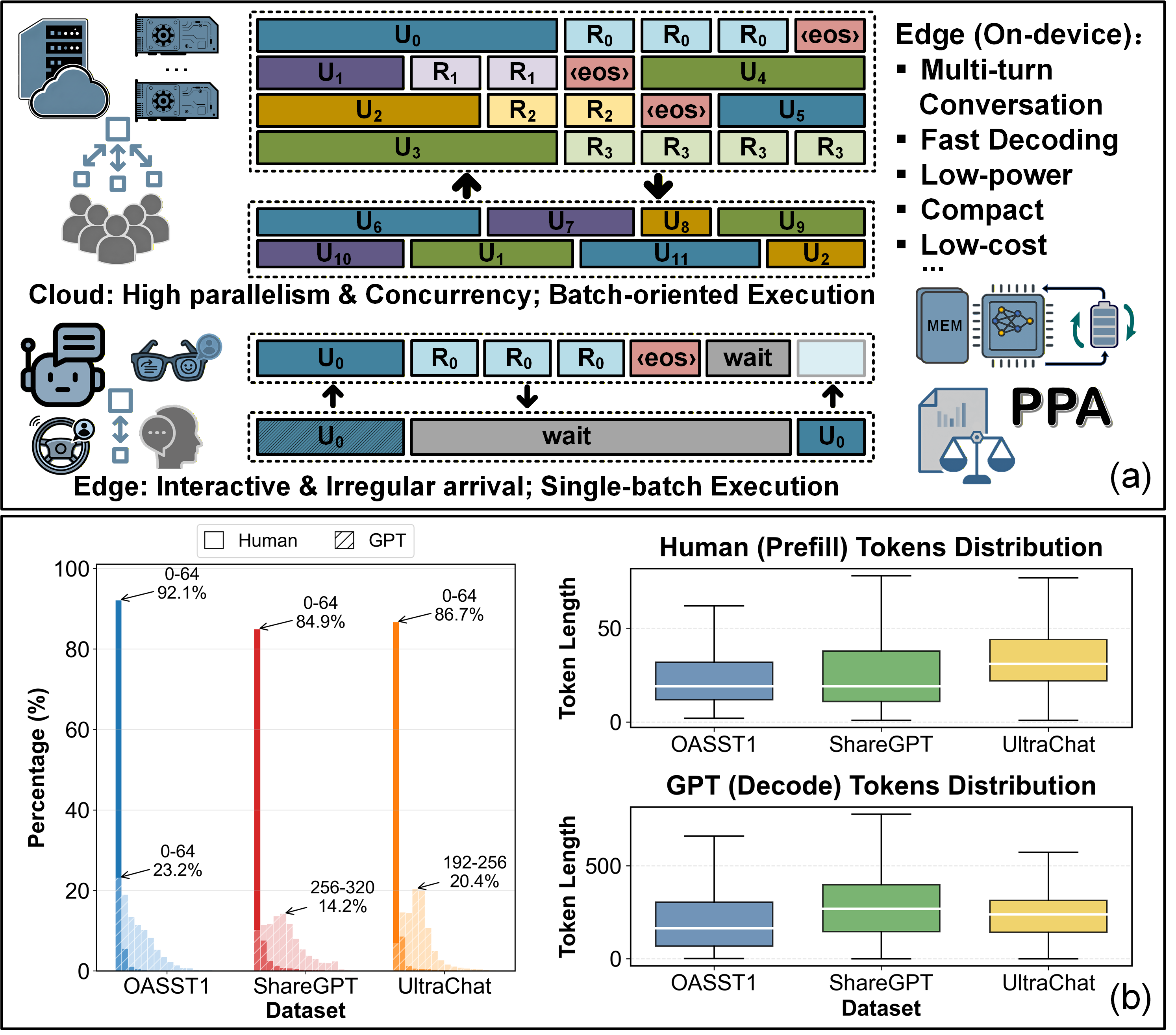
Figure 1: (a) Distinction in execution characteristics between edge and cloud LLM inference hardware. (b) Token length distribution in realistic human-LLM conversations showing the dominance of long-generation, single-batch decodes.
NVLLM targets this regime by offloading the feed-forward network (FFN) computation—a major source of parameter storage and data movement—into the NAND Flash substrate, while attention computation and KV caching remain on a lightweight CMOS-logic plus DRAM subsystem. This partition directly addresses the growing proportion of FFN parameters (e.g., ~70% in LLaMA variants) while relegating the irregular, bandwidth-hungry attention path to DRAM where it is more tractable.
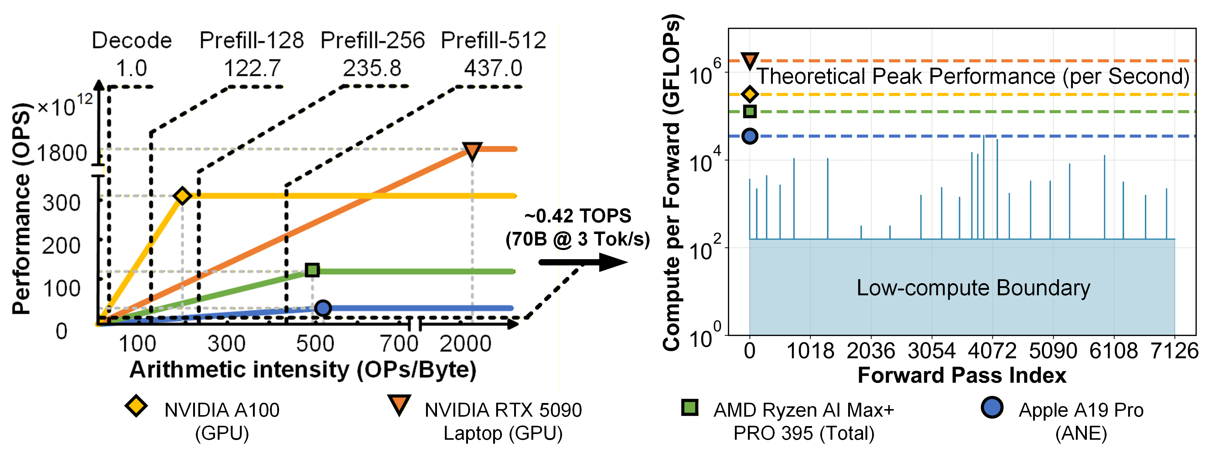
Figure 2: Under single-batch inference, hardware execution remains persistently memory-bound, even for large compute-capability devices.
NVLLM's adoption of wafer-to-wafer integration and error-resilient, out-of-order pipelining directly exploits architectural opportunities unique to 3D NAND, transforming what is traditionally a storage substrate into an active inference accelerator.
Architectural Design
Plane-Lane Co-Design and In-Flash Dot-Product Execution
FFN computation is mapped to a clustered multi-plane architecture, where wide plane clusters are tightly coupled with parallel execution lanes via co-designed FIFOs and segment buffers. This allows full-rate, direct dot-product processing on raw NAND pages, amortizing read stalls and maximizing in-situ bandwidth. Each FFN GEMM/GEMV operation is decomposed into fine-grained dot-product segments scheduled for out-of-order vector MAC execution.
Error-resiliency is achieved by decoupling error detection from correction. An in-Flash error-resilient dot-product engine (ERDPE) employs segment-level ECC, checker, and corrector units to sustain full pipeline throughput in the presence of raw bit errors typical of high-density NAND. Segments failing detection are corrected asynchronously, preventing pipeline stalls. Scoreboard-based scheduling guarantees numerical consistency, while hardware-efficient control structures minimize area and power overhead in the SRAM- and logic-constrained NAND CMOS die.
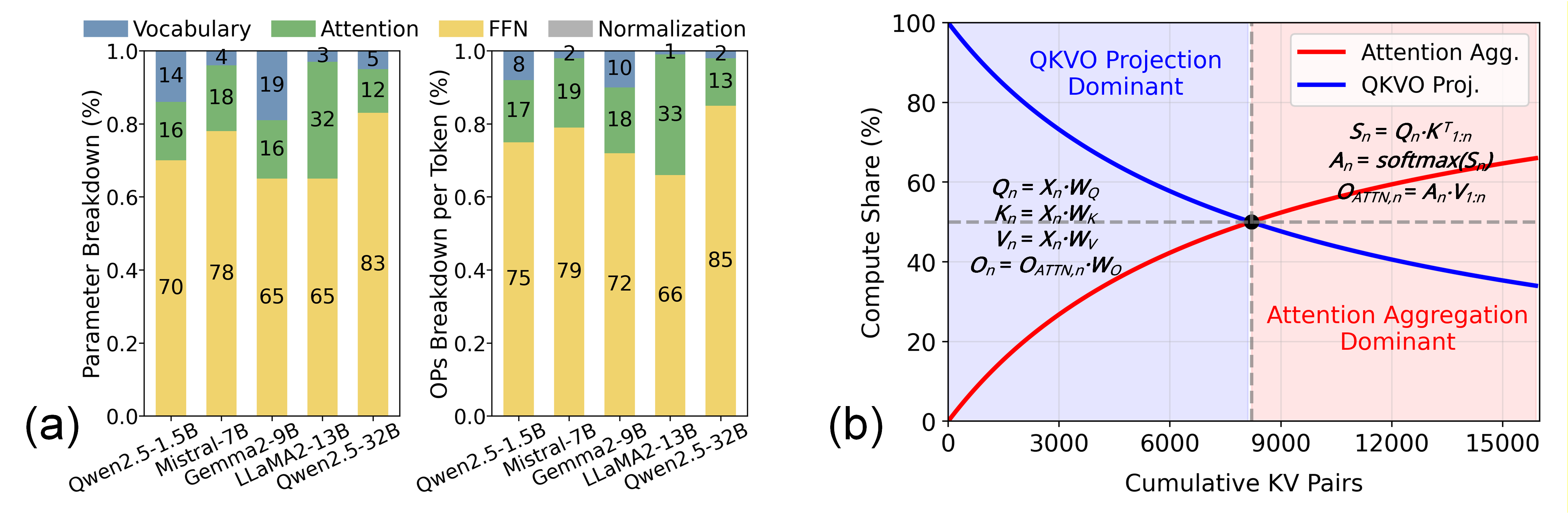
Figure 3: (a) FFN layers constitute the majority of model parameters and per-token operations. (b) Attention operation complexity grows with increasing KV-cache size.
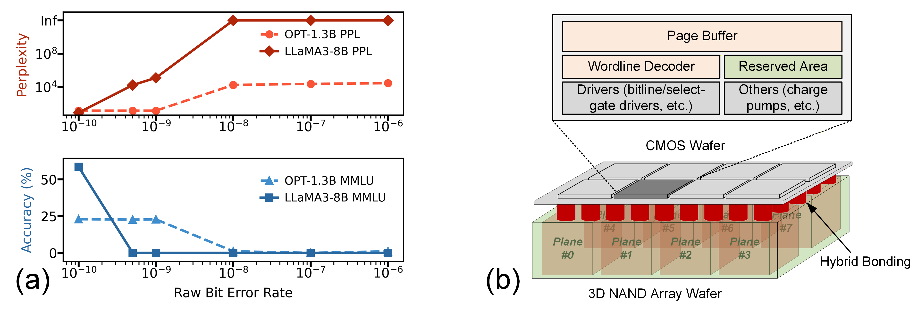
Figure 4: (a) NAND RBER directly degrades perplexity and accuracy; (b) area constraints drive the need for lightweight, error-tolerant compute pipelines in Flash.
End-to-End Dataflow and Scheduling
NVLLM employs deterministic prefetching and fine-grained pipeline scheduling to synchronize Flash array dataflows with lane-level MAC consumption. Prefetches are precisely aligned with expected activation strides and ECC check/corrector readiness, leveraging the regular access patterns of FFN computation stored in memory-dense Flash.
Attentional paths (Q/K/V/O weights, context caches) are pinned in DRAM and served by an external NPU. The global scheduler incorporates a KV-cache-aware mechanism, dynamically partitioning compute between Flash CMOS and the NPU as context length evolves. Segment-level adaptive offloading sustains high throughput and consistent per-token latency even as the attention working set size inflates with ongoing dialogue.
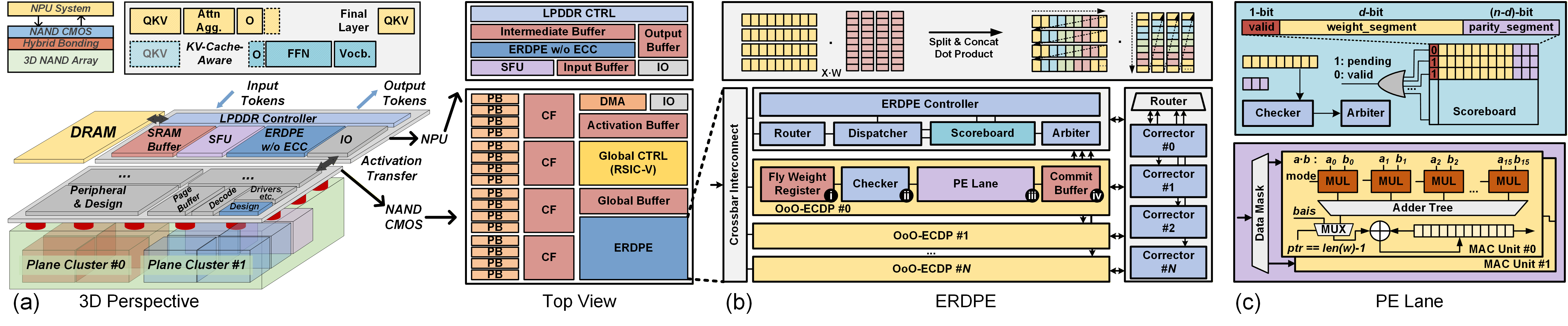
Figure 5: NVLLM architecture showing multi-plane 3D NAND clusters, ECC-enabled dot-product engines, co-optimized NPUs, and hierarchical buffering.
Quantitative Results
NVLLM exhibits strong empirical gains over both GPU-centric and contemporary SSD-like in-storage compute approaches. For quantized (INT8) OPT and LLaMA models up to 30B parameters, token throughput accelerates by 16.7×–37.9× relative to A800-based, out-of-core GPU inference. NVLLM also surpasses prior in-Flash solutions (e.g., Cambricon-LLM, AiF variants) with up to 4.7× higher throughput, primarily attributed to superior internal bandwidth and more granular error-tolerant scheduling.
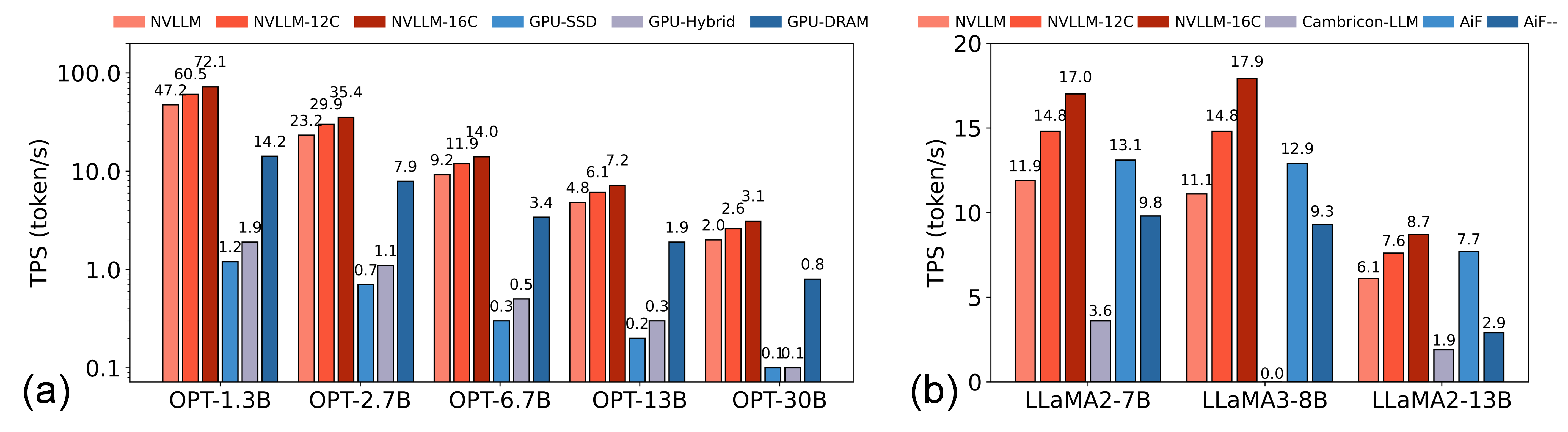
Figure 6: Throughput comparison indicates substantial speedup of NVLLM over GPU- and SSD-based architectures across multiple model scales.
End-to-end latency is reduced by up to 28.2× and scales favorably as context and decode length increase. The architectural decoupling of attention/FFN computation, combined with KV-cache-aware scheduling, allows NVLLM to sustain stable inference time distribution even as the attention cost grows.
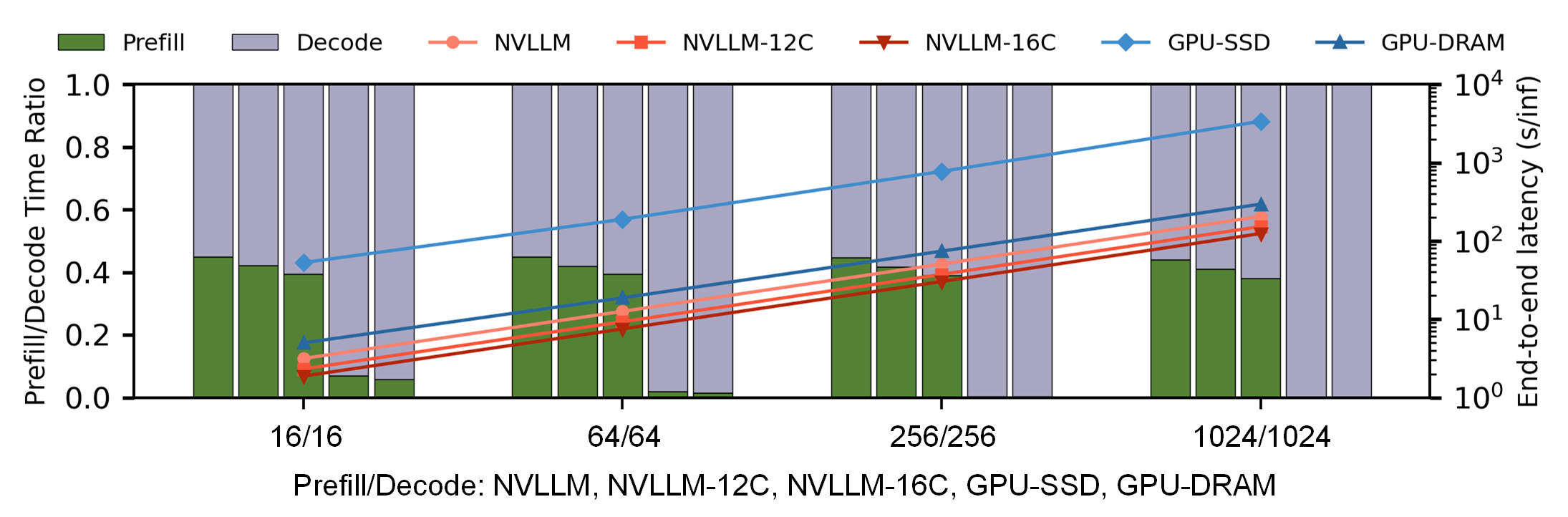
Figure 7: End-to-end latency measurements demonstrate latency improvements realized by NVLLM compared to GPU-based baselines.
Energy efficiency is also markedly improved. Data movement energy drops by 5.6× against Cambricon-LLM as model size grows, a direct outcome of keeping the bulk of FFN weights resident and processed fully within 3D NAND.
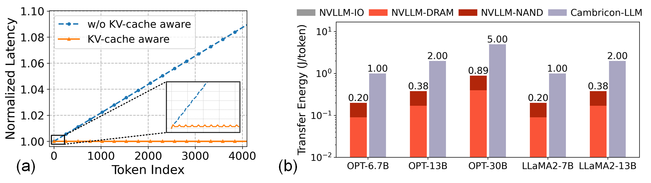
Figure 8: (a) KV-cache-aware scheduling improves throughput scalability. (b) NVLLM exhibits significantly lower energy-per-token than SSD-like in-Flash compute.
The total area impact on the NAND CMOS logic die is 2.7%, confirming the feasibility of embedding the required ECC check/corrector and datapath logic without substantial die size penalties.
Theoretical and Practical Implications
NVLLM fundamentally demonstrates that a strict hardware-software co-design exploiting regularity in FFN parameter access, tolerance to nonzero RBER, and aggressive compute/memory partitioning can overcome the dominant bandwidth limitations encountered in edge LLM inference. Efficient wafer-to-wafer stacking and lightweight, resilient execution pipelines deliver both high throughput and robustness, supporting INT8/BF16 quantization and scaling efficiently across a spectrum of multi-billion parameter models.
The architecture relaxes the reliance on costly, power-hungry DRAM scaling and enables true standalone inference on edge-class platforms. Its decoupled design both tolerates NAND-specific error patterns and flexibly meets real-world attention workload scaling via context-adaptive dynamic scheduling.
Future Prospects
NVLLM opens several avenues for research and system development:
- Broader in-storage compute: Extending this architectural template to other memory-bound neural workloads, integrating more sophisticated error-resilience for future ultra-dense NAND, and evaluating in-situ support for non-FFN blocks.
- Algorithmic scheduling: Exploring more advanced adaptive pipeline control, particularly in multi-tenant conversational agents or multi-modal LLMs, to maximize pipeline occupancy under dynamic edge constraints.
- Process technology advancements: Benefiting from the continued scaling of wafer-to-wafer bonding and denser NAND stacks, enabling further area-power reduction and substrate co-localization with SoC hosts.
Conclusion
NVLLM establishes a new paradigm in on-device LLM inference by co-optimizing 3D NAND, CMOS logic, NPU, and DRAM subsystems through principled partitioning of storage and compute. Its hybrid-bonded, error-resilient, and highly parallel architecture delivers significant advancements in throughput, latency, and energy efficiency over current GPU- and SSD-driven baselines, substantiating the practical viability of edge-class LLMs in resource-constrained environments.

