- The paper presents a spike-time learning algorithm that eliminates floating-point multiplications and explicit gradient storage for SNN training.
- The methodology employs single-spike temporal coding and an event-driven FPGA architecture to achieve competitive accuracy on benchmarks.
- The implementation on Xilinx Artix-7 FPGA reduces resource usage, enabling scalable and real-time on-chip learning for low-power edge applications.
Multiplication-Free Spike-Time Learning and Efficient FPGA Implementation for On-Chip Spiking Neural Network Training
Introduction
The paper "A Multiplication-Free Spike-Time Learning Algorithm and its Efficient FPGA Implementation for On-Chip SNN Training" (2604.23218) introduces a novel supervised learning algorithm for Spiking Neural Networks (SNNs) and an optimized FPGA architecture, designed to address the computational and hardware limitations of traditional gradient-based SNN training. The framework eliminates floating-point arithmetic and explicit gradient storage, enabling a fully event-driven, multiplier-free, and scalable on-chip training pipeline suitable for energy-constrained edge devices.
Algorithmic Design
Single-Spike Temporal Coding and Network Structure
The SNN operates with single-spike temporal coding—each neuron emits at most one spike per input, and its latency encodes information. Input data is transformed into spike times by intensity-to-latency coding, which ensures that higher input values fire earlier. Neurons are implemented as non-leaky Integrate-and-Fire (IF) units, accumulating weighted input spikes and firing once the threshold is crossed. The class decision is determined by the output neuron with the earliest spike.
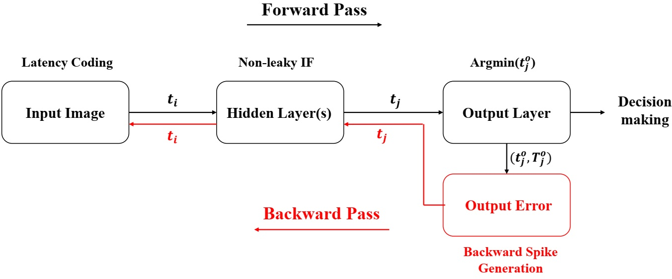
Figure 1: Proposed SNN with forward/backward spike-time propagation. Input image is encoded into spikes; backward spikes carry temporal gradients for training.
Forward Pass Mechanism
Input images are encoded into spike trains, where each spike’s timing represents its corresponding pixel intensity. IF neurons accumulate inputs in discrete time steps, producing output spikes when their membrane potential reaches threshold. The forward pass is efficiently realized with fixed-point arithmetic and parallel adder-based computations, conducive to hardware implementation.
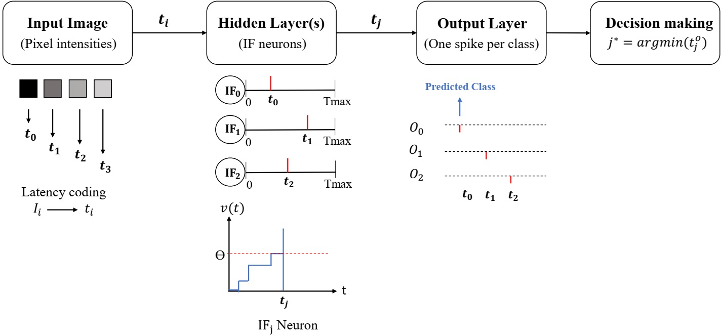
Figure 2: Forward pass of the proposed SNN, showing latency-coded input propagation and classification by earliest output spike.
Backward Pass: Spike-Time Backpropagation
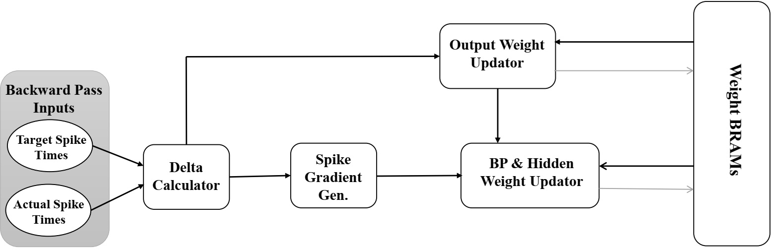
The backward pass substitutes the conventional gradient descent with a spike-time-driven backpropagation mechanism. Temporal error is defined by the difference between the actual and target spike times. Instead of propagating real-valued gradients, the method encodes delta values into backward spike times and their sign into spike polarity (positive/negative). This eliminates multiplications and centralized gradient storage. Backward spikes propagate error information purely by spike timing and sign—earlier spikes correspond to larger gradients.
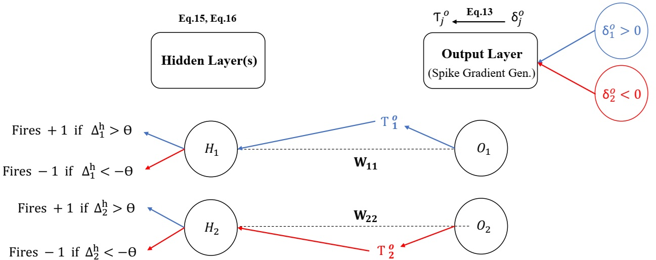
Figure 3: Spike-based gradient propagation; each neuron emits a signed backward spike determined by the sign and magnitude of its error.
Hardware Architecture and FPGA Implementation
Modular Event-Driven Design
The architecture targets Xilinx Artix-7 FPGA and comprises modular layers built around parallel non-leaky IF neurons, dedicated BRAMs for weight and spike time storage, and adder trees for efficient summation of inputs. No DSP slices are needed; all arithmetic is performed using LUTs, bit-shift, and addition, enhancing hardware efficiency and scalability.
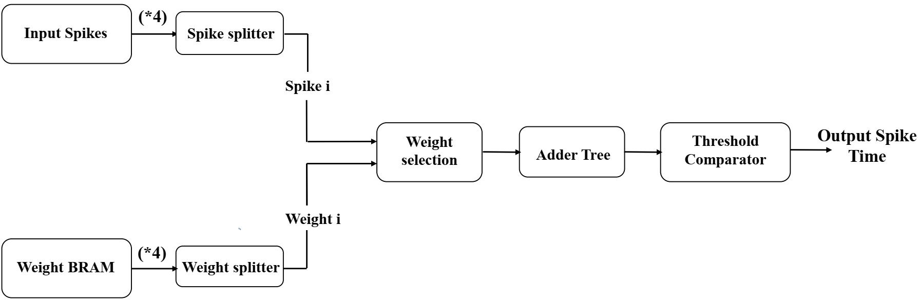
Figure 4: Schematic of a non-leaky IF neuron with parallel adder-based computations.
Multiple IF neurons are instantiated within fully connected layers for concurrent spike processing.
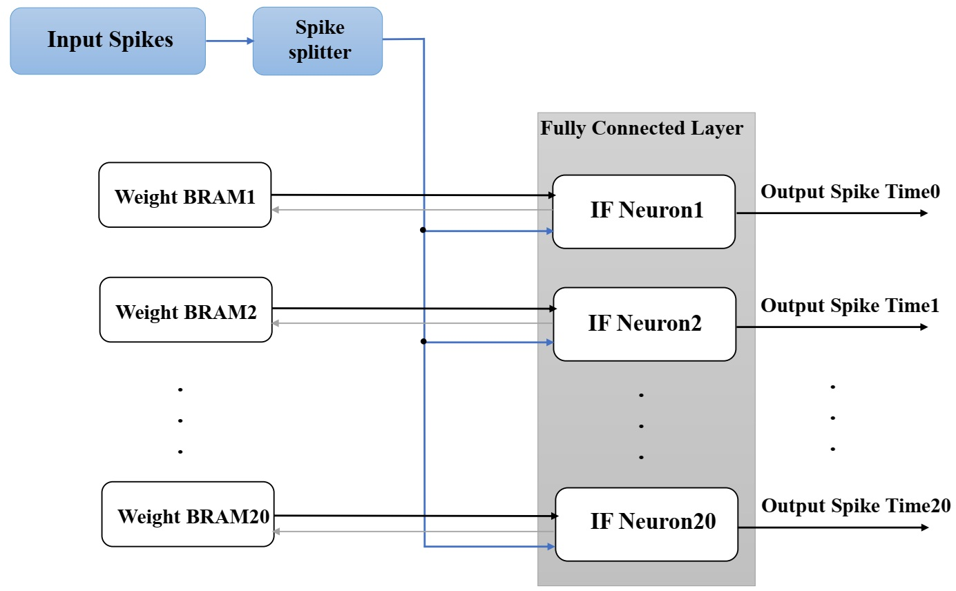
Figure 5: Fully connected layer with parallel IF neurons.
Spike-Time Backpropagation Hardware Modules
The backward pass utilizes four hardware modules:
A semi-shared FPGA architecture enables resource reuse across forward and backward passes, further minimizing hardware footprint.
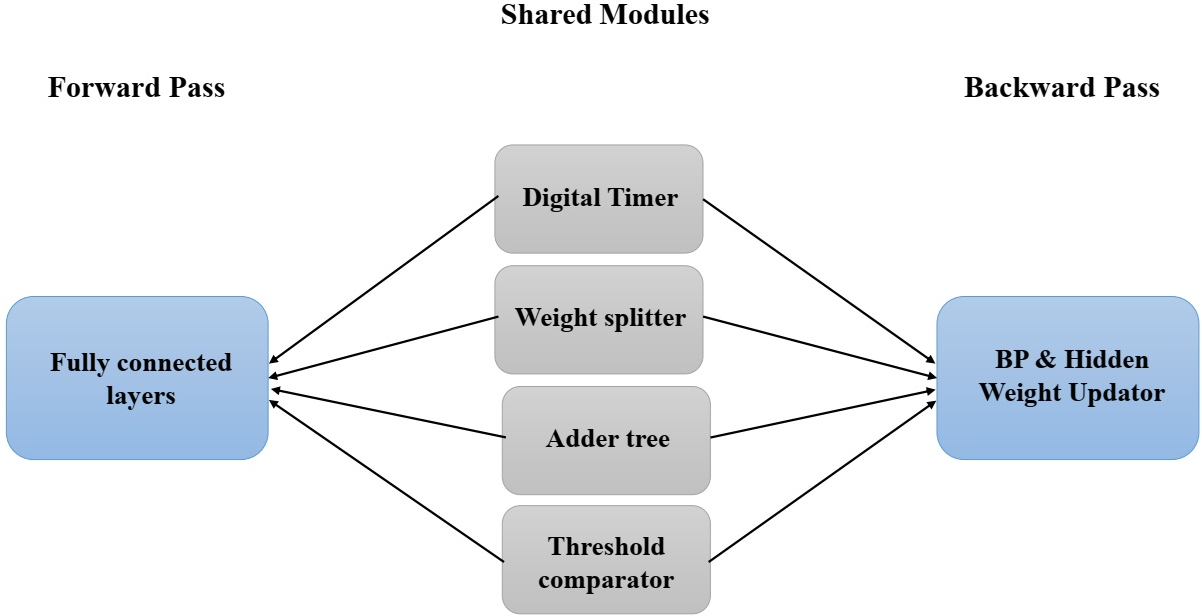
Figure 7: Semi-shared FPGA architecture, optimizing resource usage and scalability.
Universal Time Coding and Event-Driven Communication
Spike communication employs Universal Time Coding: only active spikes are transmitted with their timestamps, considerably reducing bandwidth and power consumption. Weight precision is fixed to 12-bit, and spike times are encoded with 4 bits, optimized for temporal resolution vs resource cost.
Experimental Results
The algorithm achieves competitive accuracies on standard benchmarks: 97.4% (MNIST), 84.8% (Fashion-MNIST), and up to 98% (8×8 Digits dataset), matching or closely approaching state-of-the-art SNN learning approaches such as S4NN, STiDi-BP, BS4NN, and HaSiST—all of which rely on floating-point arithmetic and/or gradient storage. The unique multiplier-free, spike-time approach does not compromise learning efficacy and generalization.
Sparsity and Computational Efficiency
Analysis shows only about 75% of synapses are active per input in the MNIST 784-400-400-10 architecture, in sharp contrast to ANNs, enhancing energy efficiency and computational sparsity.
Hardware Resource Utilization
Compared to HaSiST (rate-based, floating-point FPGA design), this approach achieves:
- Forward pass: 0.66 registers/synapse, 1.68 LUTs/synapse (vs 1.03 and 2.8 for HaSiST)
- Backward pass: 1.33 registers/synapse, 5.1 LUTs/synapse (vs 2.63 and 37.84 for HaSiST)
- No DSP slices required for either pass
This represents a roughly 7.4× reduction in LUT use and 2× reduction in registers for learning, and removes multiplication bottlenecks entirely.
Frequency and Throughput
- Forward pass: 125.5 MHz, backward pass: 105.3 MHz (2.1× faster training than HaSiST’s backward pass)
- Throughput: 0.0316×10⁹ features/sec, with real-time processing for edge applications
Implications and Future Directions
The multiplication-free SNN learning algorithm fundamentally aligns spiking computation with hardware constraints: sparse, event-driven, fixed-point arithmetic supports distributed asynchronous weight updates. By eliminating floating-point arithmetic and explicit gradient storage, the method enables scalable, real-time on-chip learning for edge and neuromorphic systems on reconfigurable platforms.
Practical implications include:
- Highly efficient SNN training on low-power FPGAs, suitable for adaptive intelligence at the edge
- No reliance on offline GPU training, unlocking real-time learning and adaptation in deployed embedded environments
- Significantly improved scalability for deep SNNs, with minimal hardware overhead and predictable timing
Theoretically, encoding gradients as spike latencies suggests new directions for biologically plausible learning mechanisms and event-driven optimization algorithms with direct hardware compatibility.
Future research will focus on advancing spike-time quantization, adaptive synchronization protocols, and architectural scaling for larger networks. Integration with more complex cognitive tasks and deployment in diverse edge scenarios are promising avenues, alongside exploration in custom ASICs and neuromorphic chips.
Conclusion
The presented spike-time-driven supervised learning algorithm and its efficient FPGA implementation demonstrate robust, high-accuracy SNN training in a fully multiplier-free, event-driven paradigm. The architectural and algorithmic innovations achieve substantial reductions in resource usage, higher processing speeds, and competitive accuracy, effectively bridging the gap between biologically inspired computation and practical neuromorphic hardware for energy-constrained environments. The approach sets the foundation for further advances in scalable, real-time, on-chip learning for deep SNNs.